High PCB quality
Defined design rules and close collaboration with audited PCB manufacturers result in layouts that can be produced with high quality and optimized costs.
Layer by layer to the perfect PCB design: TQ creates PCB layouts for demanding applications – from classic board layouts to high-density HDI designs with BGA assembly. As an E²MS system supplier, we support you throughout the entire layout process, from the netlist to the final Gerber data, always in close coordination with production and testing.
Our services in PCB design
In PCB routing, our team takes all relevant electrical, thermal, and production-related requirements into account. The layout of a printed circuit board has a decisive impact on signal integrity, EMC behavior, assemblability, testability, and the production costs of the PCB and assembly.
Anyone looking to have a printed circuit board designed is therefore in the best hands with a partner like TQ, as we take not only development, but also production and testing into account.


High-density PCB layouts with BGA and µBGA components enable the realization of highly miniaturized assemblies while maintaining a high level of functionality. TQ implements blind and buried vias as well as complex layer stack-ups in a reliable and application-specific manner. At the same time, we place particular emphasis on selecting the most suitable and cost-effective via technology and the minimum number of layers required. This ensures maximum component density and reliable signal routing, even with the finest structures.

For fast digital and RF interfaces, TQ develops impedance-controlled designs that take signal integrity and EMC requirements into account from the outset. Topics such as length matching, controlled impedances, optimized return current paths, and minimized crosstalk are implemented in a targeted manner to ensure stable data transmission even at high data rates.

TQ develops printed circuit boards for demanding power applications with maximum current density and voltages of up to several kV. The focus is on the optimal dimensioning of trace widths, suitable copper thicknesses, and compliance with standard-compliant creepage and clearance distances.

For applications with limited installation space or special mechanical requirements: TQ creates layouts for flexible and rigid-flex PCBs with particular attention to bend radii, material transitions, and mechanical reliability – ideal for compact devices, moving assemblies, or demanding installation situations.

Thermally optimized designs are crucial for the service life and reliability of printed circuit boards. TQ develops designs with targeted heat management and a suitable cooling concept and, if desired, uses thermal simulations for validation. Special technologies such as aluminum core PCBs are also used where appropriate.

Already during the PCB design phase, our layout engineers work directly in the integrated 3D environment within the ECAD tools. This enables clearance and insulation checks to be performed early in the process – not only on the PCB itself, but also in relation to the surrounding enclosure – before the assembly is manufactured.
At the same time, realistic 3D models of the electronic assemblies are created. These support visualization and significantly simplify enclosure design. The data can also be used for 3D printing prototypes.
This enables TQ to carry out PCB routing while taking mechanical conditions into account and ensures seamless further processing in mechanical design.

TQ takes all production and testing requirements into account as early as the layout stage. Design for Manufacturing and Design for Testability ensure that printed circuit boards can be produced efficiently and tested reliably. This reduces iterations, avoids costly redesigns, and shortens time to market.
Four-time winner of the PCB Design Award
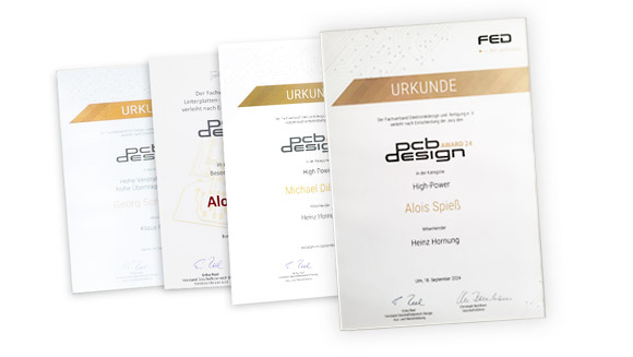
The renowned PCB Design Award from the Fachverband Elektronik-Design (FED) recognizes outstanding achievements in PCB design and highlights the key role of layout experts. TQ is among the leading award winners and has already received the award four times:
The layout process at TQ
TQ works with common professional EDA tools, including Xpedition Enterprise, Altium Designer, and PADS. Data from customer systems can usually be transferred directly.
A PCB layout designer develops the physical layout of a printed circuit board based on a circuit diagram. This involves optimally placing components, routing traces, and taking electrical and mechanical requirements into account to ensure a functional and production-ready PCB design.
TQ supports the entire PCB design process – from the netlist and PCB layout through to the final production data. Throughout the process, there is close coordination with manufacturing and test equipment development to ensure a smooth and efficient result.
Professional PCB design is crucial for complex requirements such as high-speed signals, high power density, or miniaturized assemblies. In these cases, an experienced PCB layout designer ensures that functionality, reliability, and EMC behavior are optimally implemented.
Design for Manufacturing means that the PCB layout is aligned with manufacturing requirements already during the development phase. This ensures that the printed circuit board can be produced efficiently, helps avoid errors, and shortens time to market.
To create a PCB layout, circuit diagrams, netlists, component data, and mechanical specifications are typically required. The more complete the data set, the more efficiently the PCB design and layout process can be carried out.
Yes, TQ has extensive experience in layout development for demanding applications such as HDI, high-speed, high-current, and rigid-flex designs. This allows even complex projects to be implemented reliably.